← Electric Tarp Motor Wiring Diagram: Cover with Ease! Rotary tarp switch wiring diagram Chrysler Voyager Radio Wiring Diagram: Simplify Your Repairs! Chrysler grand voyager radio wiring diagram →
If you are looking for Beginner’s Guide to PCB Design: 10 Steps to Craft Your Own Printed you've visit to the right place. We have 25 Pictures about Beginner’s Guide to PCB Design: 10 Steps to Craft Your Own Printed like Beginner’s Guide to PCB Design: 10 Steps to Craft Your Own Printed, From Schematic Diagram to PCB Layout: Simplifying the Design Process and also KiCAD 7 PCB Layout in 5 steps - YouTube. Read more:
Beginner’s Guide To PCB Design: 10 Steps To Craft Your Own Printed
 creatiwise.com
KiCAD 7 PCB Layout In 5 Steps - YouTube
 www.youtube.com
PCB Layout Support - Embizon Technologies - PCB Design Services, Bangalore
 www.embizon.com
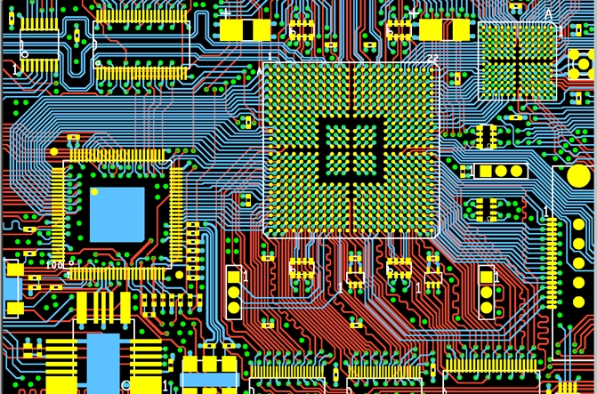
How To Design A PCB Layout - Circuit Basics
 www.circuitbasics.com
pcb layout circuits electronics campbell posted
A Step By Step Guide For PCB Designing – PsiBorg
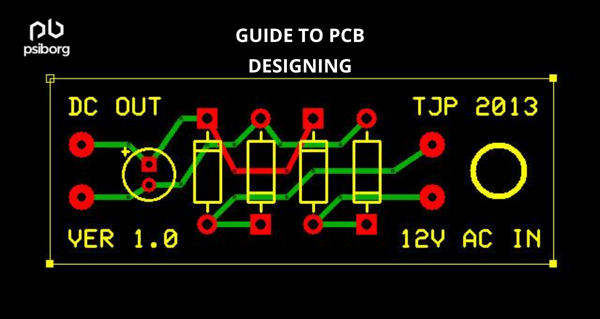 psiborgin.wordpress.com
How Do I Convert A Schematic To PCB Layout In KiCad (Step By Step
 www.raypcb.com
Altium Pcb Layout Tutorial
 wiringguideguilds.z13.web.core.windows.net
From Schematic Diagram To PCB Layout: Simplifying The Design Process
 elecschem.com
Tutorial #4: How To Do PCB Layout (Step By Step) - YouTube
 www.youtube.com
pcb
Printed Circuit Board Design, Diagram And Assembly | Steps & Tutorial
 www.electronicsandyou.com
pcb circuit santosh das circuitos impresos circuito
Pcb Design With Altium Altium Step By Step Tutorial Arduino | Sexiz Pix
 www.sexizpix.com
PCB Schematic Design - Step By Step Guide | Reversepcb
 reversepcb.com
PCB Designing: How To Design A PCB - Step By Step Guide
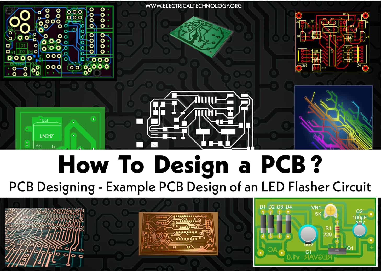 www.electricaltechnology.org
pcb design designing circuit step led board example using flasher timer
PCB Layout: A Comprehensive Guide
 www.wevolver.com
Step-by-step Cadence PCB Design Tutorial - RayMing PCB
 www.raypcb.com
Top 10 PCB Layout Tips For Beginners - HardwareBee
 hardwarebee.com
pcb
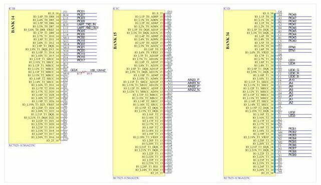
Reverse Engineering Electronic PCB Board Schematic Diagram Plan
 www.circuitwork.tech
pcb schematic antenna circuit compiling critical
How To Design A PCB Schematic: A Step-by-Step Guide
 www.mokotechnology.com
PCB Schematic Design – Step By Step Guide – PCB HERO
 www.pcb-hero.com
How To Use EasyEDA To Design PCB Schematic Step By Step
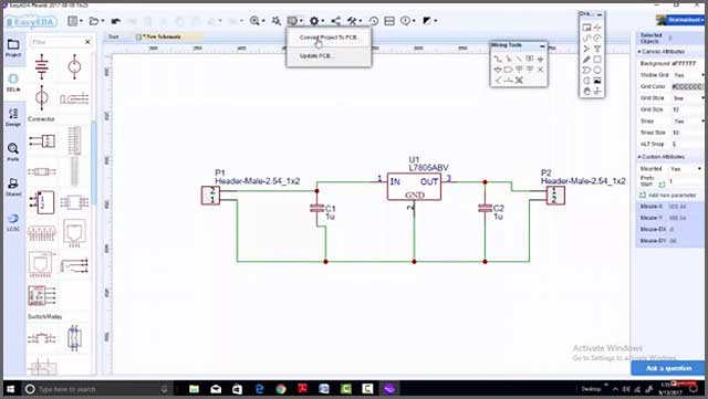 www.wellpcb.com
easyeda pcb
How To Convert Schematic Diagram Into PCB Layout? - Artist 3D
 artist-3d.com
PCB Design Layout Guidelines For Engineers | Advanced PCB Design Blog
 resources.pcb.cadence.com
Your Guide To PCB Layout Design Basics & Steps | Viasion
 www.viasion.com
Basic Steps To Design A PCB Layout – PCB HERO
 www.pcb-hero.com
How To Design A PCB Layout - Circuit Basics
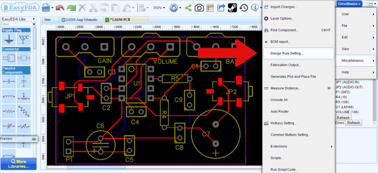 www.circuitbasics.com
pcb layout circuitbasics
Pcb schematic design. How to convert schematic diagram into pcb layout?. Pcb designing: how to design a pcb